|
MetaLaser INC.
|

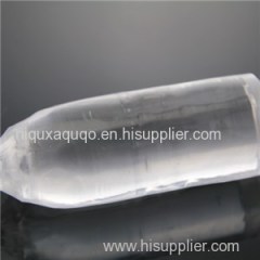
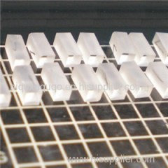
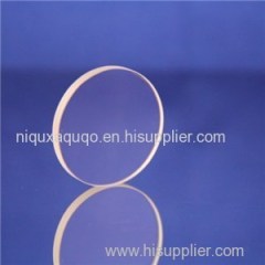
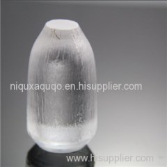
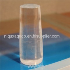
Ce YAP Scintillation Detector
| Place of Origin: | , China (Mainland) |
|
|
|
| Add to My Favorites | |
| HiSupplier Escrow |
Product Detail
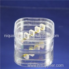
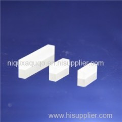
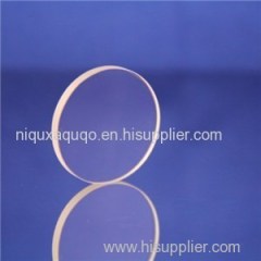
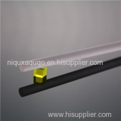
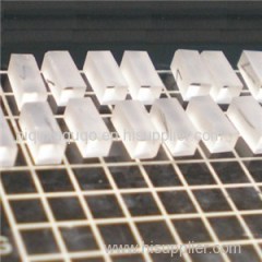
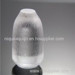
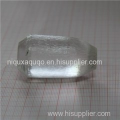
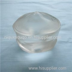
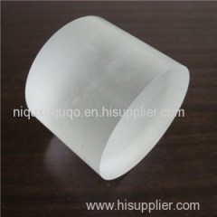
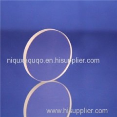
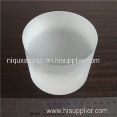
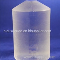
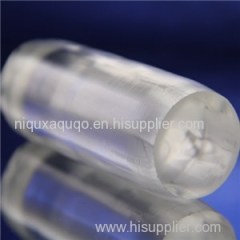
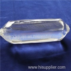
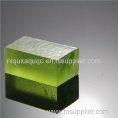
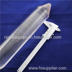
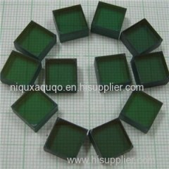
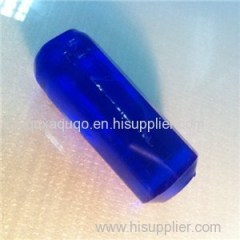
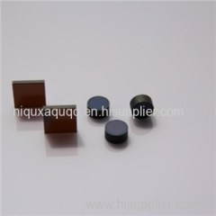
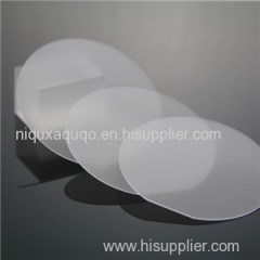
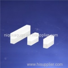
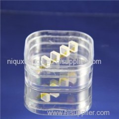
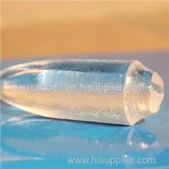
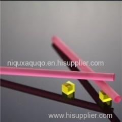
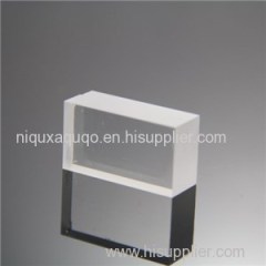
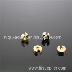
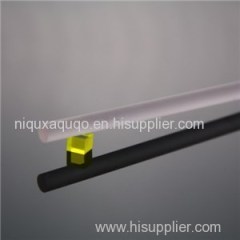
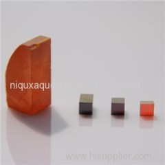
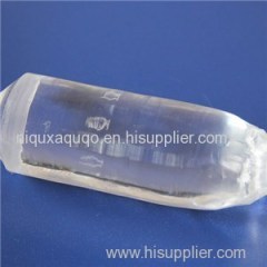
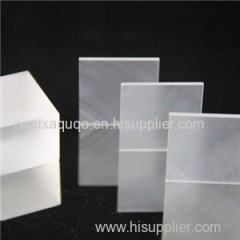
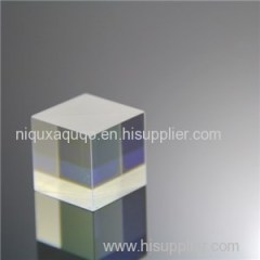
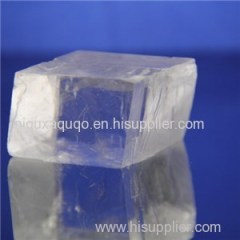
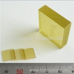
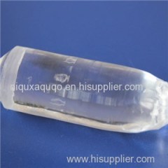
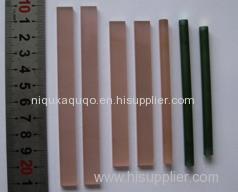
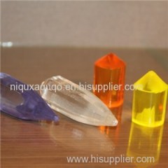
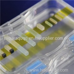
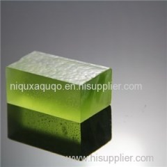
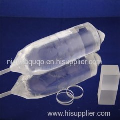
Ce YAP Scintillation Detector,Scintillation Detector
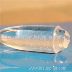
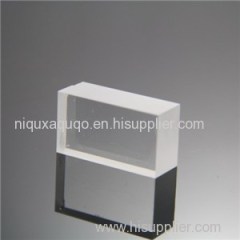
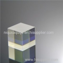
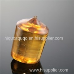
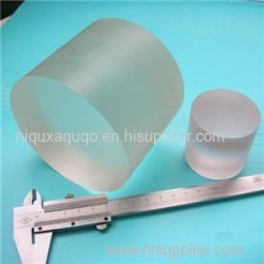
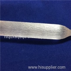
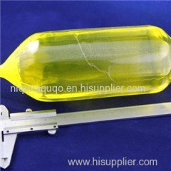
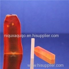
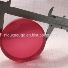
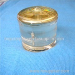
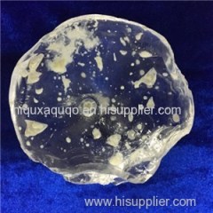
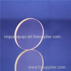
DescriptionYttrium aluminum perovskite activated by cerium(Cerium doped yttrium aluminum,Website:http://www.meta-laser.com, Ce-doped YAlO3,Ce:YAG) is a fast, mechanically strong and chemically resistant scintillation material. Mechanical properties enable precise machining and entrance windows can be made with a very thin aluminum layer deposited directly on the entrance surface of the crystal. Ce:YAP scintillators have very low energy secondary X-ray emissions which makes them desirable for imagining applications. Ce:YAP detectors are used for gamma and X-ray counting, electron microscopy, electron and X-ray imaging screens, and tomography systems.SpecificationParameters of materialsMaterialsCe:YAPMohs Hardness8.5Melting Point1875°Refractive Index1.97Density5.37Polishing Specification for Optical GradeⅠOrientation Tolerence< 1°Thickness/Diameter Tolerance±0.10 mmSurface Flatness<(λ-2λ)@632nmWavefront Distortion<(2-4)λ@632nmSurface Quality80/50Parallel10ˊPerpendicular60ˊClear Aperture>90%Chammfer<0.2×45°Polishing Specification for Optical Grade ⅡOrientation Tolerence< 0.5°Thickness/Diameter Tolerance±0.10 mmSurface Flatness<(λ/2-λ/4)@632nmWavefront Distortion<(1-2)λ@632nmSurface Quality60/40Parallel1ˊPerpendicular30ˊClear Aperture>90%Chammfer<0.2×45°Polishing Specification for Optical Grade ⅢOrientation Tolerence< 0.2°Thickness/Diameter Tolerance±0.02 mmSurface Flatness(λ/4-λ/6)@632nmWavefront Distortion<(λ-λ/2)@632nmSurface Quality40/20Parallel45〞Perpendicular20ˊClear Aperture>90%Chammfer<0.2×45°Standard productsProductConcentrationAperture dimensions,mmlength,mmProduct IDPriceCe:YAP0.01%-0.8%0-550.1-120 Polishing Specification for Optical GradeⅠOrientation Tolerence< 1°Thickness/Diameter Tolerance±0.10 mmSurface Flatness<(λ-2λ)@632nmWavefront Distortion<(2-4)λ@632nmSurface Quality80/50Parallel10ˊPerpendicular60ˊClear Aperture>90%Chammfer<0.2×45°Polishing Specification for Optical Grade ⅡOrientation Tolerence< 0.5°Thickness/Diameter Tolerance±0.10 mmSurface Flatness<(λ/2-λ/4)@632nmWavefront Distortion<(1-2)λ@632nmSurface Quality60/40Parallel1ˊPerpendicular30ˊClear Aperture>90%Chammfer<0.2×45°Polishing Specification for Optical Grade ⅢOrientation Tolerence< 0.2°Thickness/Diameter Tolerance±0.02 mmSurface Flatness(λ/4-λ/6)@632nmWavefront Distortion<(λ-λ/2)@632nmSurface Quality40/20Parallel45〞Perpendicular20ˊClear Aperture>90%Chammfer<0.2×45°Key parameter1.Transmittance graph 2.Luminescence spectra of Ce:YAP crystals3. Pulsed x ray excited and emitted decay curve
Related Search
Ce Approved
Adapter With Ce
Detector
Ce Electric Scooter
Ce Electric Bicycle
Ce Electric Bike
More>>
Find more related products in following catalogs on Hisupplier.com
Company Info
MetaLaser INC. [China (Mainland)]
Business Type:Manufacturer
City: Nanjing
Province/State: Jiangsu
Country/Region: China (Mainland)